以TMS320F28030为例,其它型号可能有差异,不过大同小异。
在TI C2000 DSP中,PWM模块是一个独立的模块,并没有算作通用定时器的一部分,这也充分体现了C2000系列用于控制系统的定位。整个ePWM模块可以视为由若干个独立的ePWM子模块组成,每个ePWM子模块对应2个互补输出的通道——EPWMxA及EPWMxB。这样的设计减少了各PWM通道间的耦合关系,使用起来更为方便灵活。
在TI的参考手册中是这样说的:
Cross coupling or sharing of resources has been avoided; instead, the ePWM is built up from smaller single channel modules with separate resources that can operate together as required to form a system. This modular approach results in an orthogonal architecture and provides a more transparent view of the peripheral structure, helping users to understand its operation quickly.
各独立的ePWM模块可以单独工作,也可以通过时钟同步策略来连接为一个整体,除此之外,时钟同步还可用于同步ePWM模块与eCAP模块。下文所说的ePWM模块都是指每个独立的子模块。
概述
ePWM模块的简要结构框图如下: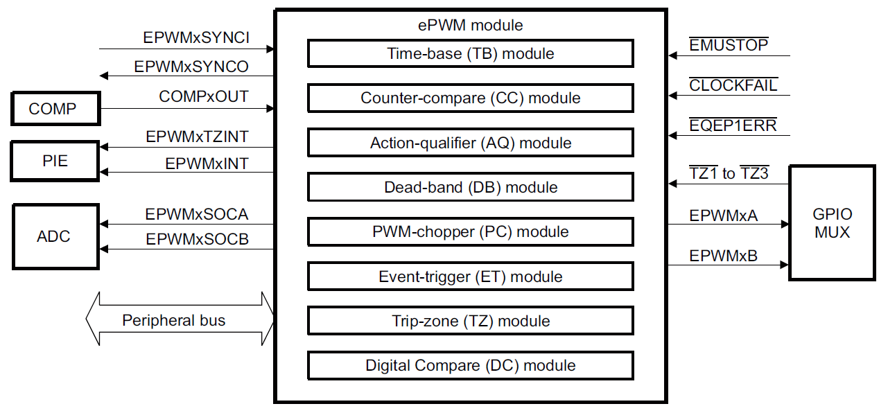
- 输出信号:
** EPWMxA & EPWMxB :**
PWM信号输出。
** EPWMxTZINT & EPWMxINT :**
中断信号输出,连接至PIE模块。
** EPWMxSOCA & EPWMxSOCB :**
ADC SOC信号输出,用于控制ADC开始进行数据转换的时间。
Each ePWM module has two ADC start of conversion signals . Any ePWM module can trigger a start of conversion . Which event triggers the start of conversion is configured in the Event-Trigger submodule of the ePWM.
- 输入信号:
** TZ1 ~ TZ6 :**
错误信号输入,ePWM模块内部可以选择性的处理这些错误信号,具体含义:
These input signals alert the ePWM module of fault conditions external to the ePWM module. **Each module on a device can be configured to either use or ignore any of the trip-zone signals. The TZ1 to TZ3 trip-zone signals can be configured as asynchronous inputs through the GPIO peripheral. TZ4 is connected to an inverted EQEP1 error signal (EQEP1ERR) from the EQEP1 module (for those devices with an EQEP1 module). TZ5 is connected to the system clock fail logic, and TZ6 is connected to the EMUSTOP output from the CPU. **This allows you to configure a trip action when the clock fails or the CPU halts.
** COMPxOUT :**
比较器模块的输出信号。
- 时钟同步信号:
** EPWMxSYNCI & EPWMxSYNCO :**
菊花链结构的时钟同步信号,EPWMxSYNCI是输入,EPWMxSYNCO是输出.
各模块的连接关系见下图: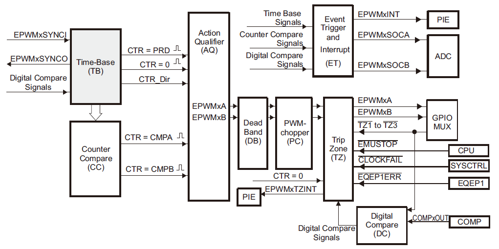
下面简要总结下各模块的核心内容,具体参考TI的Reference manual.
Time-Base
主时基模块。
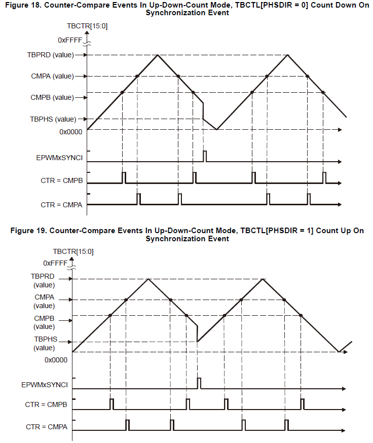
一共有3种计数方式,示意图及频率计算方法如下: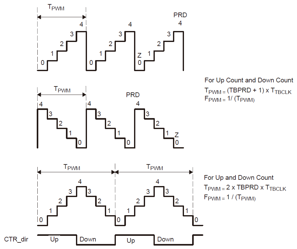
模式选择通过TBCTL[CTRMODE]位,预分频可通过TBCTL[HSPCLKDIV]位。
产生CTR = PRD及CTR = Zero这两个信号。
TBPDR寄存器有一个影子寄存器(Shadow Register),通过TBCTL[PRDLD]位来控制是否使用此功能。
The TBPRD shadow register is enabled when TBCTL[PRDLD] = 0. Reads from and writes to the TBPRD memory address go to the shadow register. The shadow register contents are transferred to the active register (TBPRD (Active) ← TBPRD (shadow)) when the time-base counter equals zero (TBCTR = 0x0000). By default the TBPRD shadow register is enabled.
时钟同步的结构见下图:
使能时钟同步的步骤如下:
The proper procedure for enabling ePWM clocks is as follows:
- Enable ePWM module clocks in the PCLKCRx register
- Set TBCLKSYNC= 0
- Configure ePWM modules
- Set TBCLKSYNC=1
注:TBCLKSYNC位位于PCLKCR0寄存器中,属于”System Control and Interrupts”的一部分。
When TBCLKSYNC = 1, all ePWM time-base clocks are started with the rising edge of TBCLK aligned. For perfectly synchronized TBCLKs, the prescaler bits in the TBCTL register of each ePWM module must be set identically
收到同步信号后:
The value of the phase register is loaded into the counter register when an input synchronization pulse is detected (TBPHS → TBCTR).
In up-down-count mode, the TBCTL[PSHDIR] bit configures the direction of the time-base counter immediately after a synchronization event. The new direction is independent of the direction prior to the synchronization event.
多个ePWM模块之间可以存在一个精确的相位差,在一些特殊的电力电子拓扑结构中特别有用。例如在大功率的应用中,对于移相变压器、多绕组变压器等,其输入有多个整流单元,相位互差特定的角度,此时就可以使用TBPHS寄存器来调整它们之间载波的相位差;而且因为是相对于同一个时间基准来计数,其精度也较高。在这种使用情况下,一般将一相ePWM做为主模块,其时钟信号作为同步源,其余几相ePWM做为从模块,其时钟信号使用同步源与TBPHS的和或者差。
Counter-Compare
计数器比较模块。
产生CTR = CMPA及CTR = CMPB这两个信号: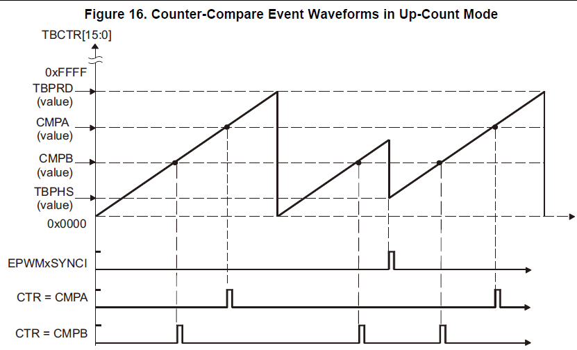
同样,CMPA与CMPB寄存器也有其影子寄存器,分别通过CMPCTL[SHDWAMODE]与CMPCTL[SHDWBMODE]来进行控制。
If the shadow register is enabled then the content of the shadow register is transferred to the active register on one of the following events as specified by the CMPCTL[LOADAMODE] and CMPCTL[LOADBMODE] register bits:
- CTR = PRD: Time-base counter equal to the period (TBCTR = TBPRD).
- CTR = Zero: Time-base counter equal to zero (TBCTR = 0x0000)
- Both CTR = PRD and CTR = Zero
Action-Qualifier
输出波形产生及控制模块。
模块原理框图: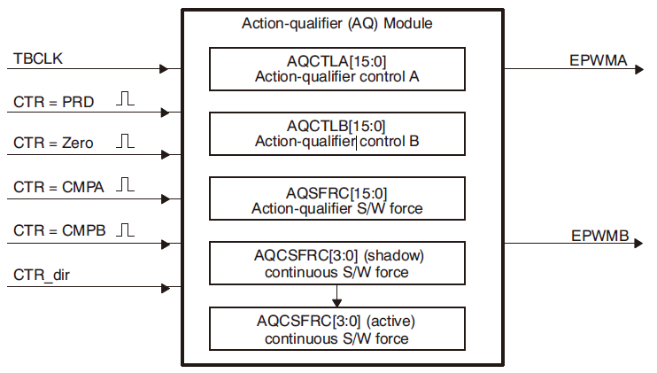
一共有4种可选操作:
- Set High : Set output EPWMxA or EPWMxB to a high level.
- Clear Low : Set output EPWMxA or EPWMxB to a low level.
- Toggle : If EPWMxA or EPWMxB is currently pulled high, then pull the output low. If EPWMxA or EPWMxB is currently pulled low, then pull the output high.
- Do Nothing : Keep outputs EPWMxA and EPWMxB at same level as currently set. Although the “Do Nothing” option prevents an event from causing an action on the EPWMxA and EPWMxB outputs, this event can still trigger interrupts and ADC start of conversion.
在寄存器AQCTLA及AQCTLB中进行配置,各种常用配置的示例代码在参考手册中有详细说明。
Dead-Band Generator
互补PWM产生及死区控制模块。
只使用Action Qualifier模块,通过灵活配置CMPA与CMPB寄存器,一样可以实现死区控制功能,然而这样做较为麻烦,更常规的做法是使用Dead Band Generator来生成互补PWM信号及控制死区时间。
模块原理框图如下: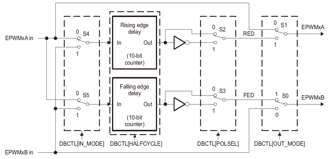
常用的配置如表,其中Mode 2 & Mode 3为最为常用的互补输出模式。(表中均为S4 = 0, S5 = 0)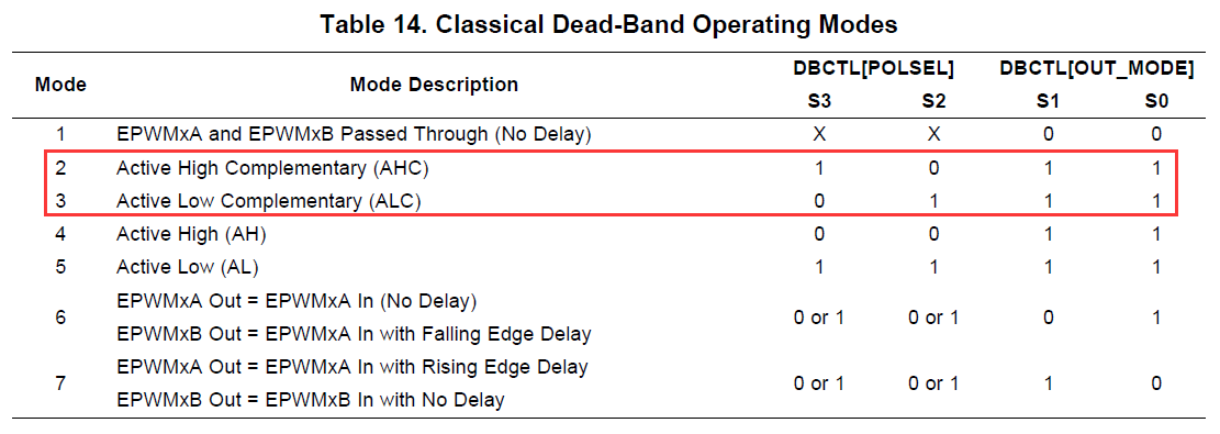
从中可以看到,在使用Dead Band Generator来生成互补PWM信号时,只使用了Action Qualifier产生的一路PWM信号,即EPWMxA,另一路信号EPWMxB并没有使用,而是根据EPWMxA来产生的。
最终生成的互补PWM信号波形如图所示:
RED及FED时间由DBRED及DBFED寄存器决定,计算方法及一些常用值见参考手册中的说明。
PWM-Chopper
斩波模块,用于在PWM输出中加入一个高频载波信号。
这个模块是可选的,其作用是用一个高频信号(最高为系统时钟的8分频)来调制PWM信号。经过调制后的输出波形效果如下: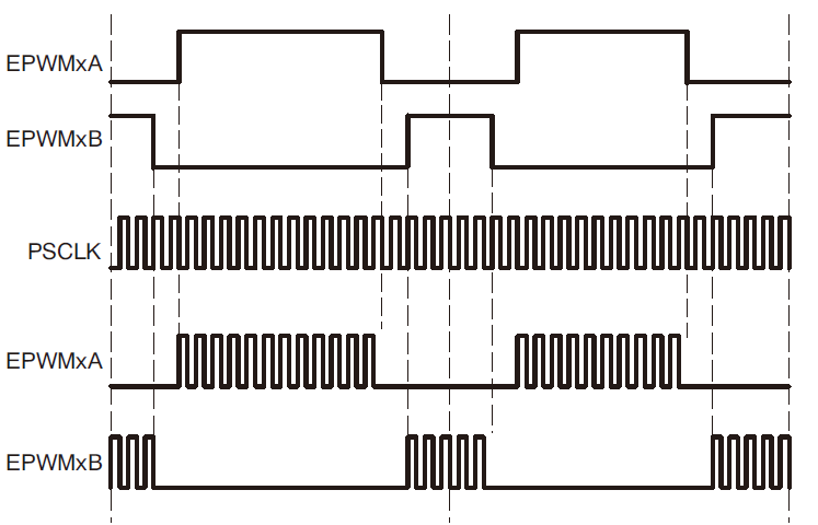
如此调制一般是用于高频开关电源中,当PWM的周期较长,用高频变压器作驱动器,就会达不到目的,并有可能烧坏器件。使用PWM-Chopper模块可以将PWM波经过“再调制”后的高频波作驱动就可以解决这个问题。
Trip-Zone
错误信号控制模块。
TZSEL寄存器选择启用哪些错误信号(TZ1~TZ6),TZCTL寄存器选择相应的操作,有4种可选操作:
- 强制拉低
- 强制拉高
- 高阻输出
- 保持原状态(Do nothing)
错误输入一共有两种模式:One-Shot(OSHT)及Cycle-by-Cycle(CBC)模式,其区别在于:
The one-shot trip condition remains latched until the user clears the condition via the TZCLR register.
A cycle-by-cycle trip condition is automatically cleared when the time-base counter reaches zero.
简而言之,就是One-Shot模式需要手动复位,而Cycle-by-Cycle模式会自动复位。
同时,Trip-Zone模块也可以产生中断,通过TZEINT寄存器来配置。
Event-Trigger
中断及外部事件触发模块。
原理框图如下: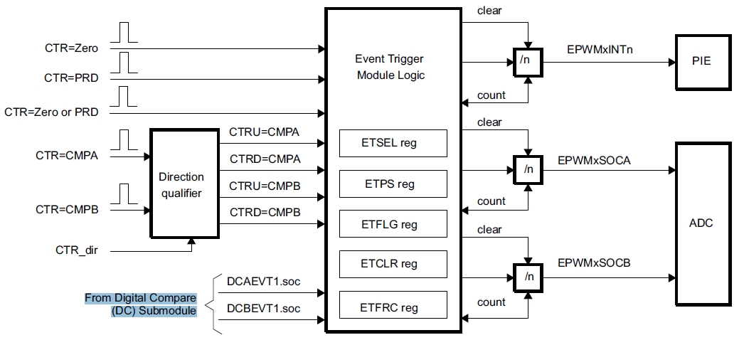
输入信号可通过ETPS[INTCNT]位配置为不产生中断、每次都产生中断、每2次产生中断、每3次产生中断。
除了中断外,还可以产生ADC模块的SOC信号。
Digital Compare
数字比较模块
原理框图如下: